Cost-effective and efficient methods for converting sunlight into electricity are the focus of green energy research. Solar cells developed for this purpose are currently made of semiconductors such as silicon. Electrical energy is generated at the junction between two different semiconductors. However, the efficiency of these solar cells has almost reached its theoretical limit. New methods of converting sunlight into electricity must be found if solar energy is to be used as a major source of electricity. An international research team from Germany, Japan and Israel has now made important progress in this direction. Zhang and colleagues recently published their findings in the prestigious journal Nature. They demonstrate a transition-free solar cell that can be made by applying a more atomic semiconductor layer into a nanotube.
In a conventional solar cell, two regions of a semiconductor are doped with different chemical elements. The electrical current is generated by the negatively charged electrons of a region and by the positively charged electron holes (holes). At the junction between these two areas, an electric field is created. When sunlight is absorbed at this junction, electron-hole pairs are formed. The electrons and holes are then separated by the resulting electric field, generating an electric current. This conversion of solar energy into electricity is called photovoltaic effect. This photovoltaic effect is particularly important for green energy production. Its efficiency has almost reached the theoretical limit as mentioned above.
In technical terms, the photovoltaic effect occurs at traditional pn junctions, where a p-type material (with an excess of holes) adjoins an n-type material (with an excess of electrons). Current is generated in the photo-induced generation of electron-hole pairs and their subsequent separation. Further advances are expected through the use of other photovoltaic effects that do not require transition and only occur in crystals with broken inversion symmetry. However, the practical implementation of these effects is impeded by the low efficiency of the materials. Semiconductors with reduced dimensionality or smaller band gap have shown to be more efficient. Transition metal dichalcogenides (TMDs) are, for example, two-dimensional small-bandgap semiconductors in which various effects were observed by breaking the inversion symmetry in their bulk crystals.
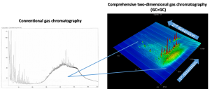
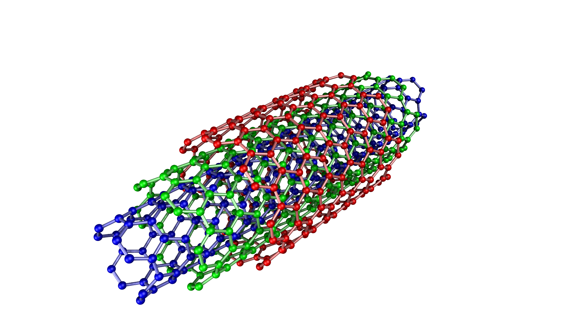
The reported bulk photovoltaic effect (BPVE) is based on tungsten disulfide, a member of the TMD family. Crystals of this material have a layered structure and can be stratified in layers similar to graphite. The resulting atomic sheets can then be rolled into tubes of 100 nanometers by chemical methods. The authors produced photovoltaic devices from three types of tungsten disulfide: a monolayer, a bilayer and a nanotube.
A systematic reduction in crystal symmetry has been achieved beyond mere fractional symmetry inversion. The transition from a two-dimensional monolayer to a nanotube with polar properties has been significantly improved. The photovoltaic current density produced is orders of magnitude greater than that of other comparable materials. The results not only confirm the potential of TMD-based nanomaterials, but also the importance of reducing crystal symmetry for improving the BPVE.
While the nanotube devices had a large BPVE, the single-layer and two-layer devices produced only a negligible electric current under illumination. The researchers attribute the different performance characteristics of the solar cells to their pronounced crystal symmetry. This way, one can spontaneously generate a current in uniform semiconductors, without a transition.
The BPVE was first observed in 1956 at Bell Labs, New Jersey, just two years after the invention of modern silicon solar cells. The effect is limited to non-centrosymmetric materials characterized by a lack of symmetry in spatial inversion. That is, the combination of a 180° rotation and a reflection. The effect has two attractive properties: the current generated by light depends on the polarization of the incident light and the associated voltage is greater than the band gap of the material. This is the energy required to excite conducting free electrons. However, the effect typically has a low conversion efficiency and was therefore of rather academic than industrial interest.
To achieve high efficiency, a photovoltaic material must have high light absorption and low internal symmetry. However, these two properties usually do not exist simultaneously in a given material. Semiconductors that absorb most of the incident sunlight generally have high symmetry. This reduces or even prevents the effect. Low-symmetry materials, such as perovskite oxides, absorb little sunlight due to their large band gap. To circumvent this problem, efforts have been made to improve light absorption in low-symmetry materials, for example by using the mentioned doping. Meanwhile, it has been shown that the effect can occur in semiconductors by using mechanical fields to adjust the crystal symmetry of the material.
The newly discovered solution is encouraging with regard to the production of high absorption semiconducting nanotubes. In the case of tungsten disulfide, the crystal symmetry of the nanotubes is reduced compared to the mono- and bilayers due to the curved walls of the tube. The combination of excellent light absorption and low crystal symmetry means that the nanotubes have a significant photovoltaic effect. The current density exceeds that of materials which are inherently low in symmetry. Nevertheless, the conversion efficiency achieved is still much lower than that of the photovoltaic effect in conventional junction-based solar cells.
The authors’ findings demonstrate the great potential of nanotubes in solar energy production and raise various technological and scientific challenges. From an application’s perspective, it would be useful to produce a solar cells that consists of a large arrays of semiconductor nanotubes to check whether the approach is scalable. The direction of the generated current would be largely determined by the internal symmetry of the material. Therefore, uniform symmetry across the nanotube array would be required to create a collective current. These currents could cancel each other out.
At Frontis Energy, we wonder if the method described could work with the classic photovoltaic effect in the same solar cell. That would possibly increase overall efficiency. The two effects could use the solar energy consecutively. Despite the remaining challenges, the presented work offers a possibility for the development of highly efficient solar cells.
(Photo: Wikipedia)