Posted on

Production of Green Hydrogen through exposure of nano particles to sunlight

The demand for energy is increasing and raw material for the fossil fuel economy is diminishing. Moreover, the emission of gases from fossil fuel usage significantly degrades air quality. The carbon by-products produced from these fossil fuels severely affect the climate.

Hence, there is a need to find a renewable energy resource, that can be produced, stored, and used easily as per requirement. Hydrogen can be a promising energy resource as it is an abundantly available, non-toxic resource, and can be readily used to store excess electrical energy.

Hydrogen when combined with oxygen in a fuel cell produces electricity and the by-products obtained are water and heat. Based on the method of production of hydrogen it is categorized as blue hydrogen and green hydrogen. Blue hydrogen is produced from fossil fuels such as methane, gasoline, coal while green hydrogen is produced from non-fossil fuels / water. The cleanest way to produce eco-friendly hydrogen is via electrolysis of water where water is electrolyzed to separate hydrogen and oxygen. Renewable energy can be used as a power electrolyzer to produce hydrogen from water. Solar driven photo electrochemical (PEC) water splitting is one of the common method used these days. In photo electrochemical (PEC) water splitting, hydrogen is produced from water using sunlight.

PEC cells comprise of a working photoelectrode and a counter electrode. The photoelectrode consists of semiconductor material with a band gap to absorb solar light and generate an electron-hole pair. The photo-generated charges are responsible for the oxidation of water and its reduction into hydrogen. The PEC suffer devices from low stability and efficiency.

The research team from the  Institut national de la recherche scientifique (INRS) along with researchers from the Institute of Chemistry and Processes for Energy, Environment and Health (ICPEES) , a CNRS-University of Strasbourg joint research lab published a way to significantly improve the efficiency of water dissociation to produce hydrogen by the development of sunlight photosensitive-nanostructured electrodes.

A comparative study between cobalt and nickel oxide nanoparticles deposited onto TiO 2 nanotubes prepared through anodization was carried out. The TiO 2 nanotubes were decorated with CoO (cobalt oxide) and NiO (nickel oxide) nanoparticles using the reactive pulsed laser deposition method. The surface loadings of CoO or NiO nanoparticles were controlled by the number of laser ablation pulses. The efficiency of CoO and NiO nanoparticles as co-catalysts for photo-electrochemical water splitting was studied by cyclic voltammetry, under both simulated sunlight and visible light illuminations and by external quantum efficiency measurements

The entire research work was carried out in the following steps:

Catalyzed Green Hydrogen synthesis
Steps followed to improve the efficiency of hydrogen production

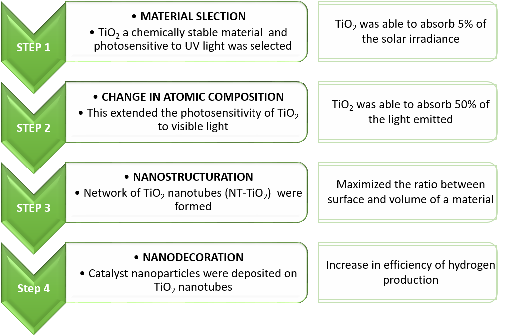
(Source: Favet et al ., Solar Energy Materials and Solar Cells , 2020)

In this study Cobalt (CoO) and Nickel (NiO) oxides were considered as effective co-catalysts for splitting water molecules. Both co-catalysts improved photo-electrochemical conversion of ultra violet as well visible light photons.

However, CoO nanoparticles were found to be the best co-catalyst under visible light illumination, with a Photo Conversion Efficiency almost 10 times higher than for TiO 2 . The performance of CoO nanoparticles got enhanced in the visible spectral region (λ> 400 nm). The possible reason can be a consequence of their visible bandgap which enables them to harvest more photon in the 400-500 nm range and transferring effectively the photo-generated electrons to TiO 2 nanotubes.

At Frontis Energy we are exited about these new discovery to improve hydrogen production from sunlight and hope to see an industrial application soon.

(Image: Engineersforum)

Reference: Favet et al ., Solar Energy Materials and Solar Cells , 2020

Posted on

Semiconductive nanotubes with photovoltaic effect

Cost-effective and efficient methods for converting sunlight into electricity are the focus of green energy research. Solar cells developed for this purpose are currently made of semiconductors such as silicon. Electrical energy is generated at the junction between two different semiconductors. However, the efficiency of these solar cells has almost reached its theoretical limit. New methods of converting sunlight into electricity must be found if solar energy is to be used as a major source of electricity. An international research team from Germany, Japan and Israel has now made important progress in this direction. Zhang and colleagues recently published their findings in the prestigious journal Nature. They demonstrate a transition-free solar cell that can be made by applying a more atomic semiconductor layer into a nanotube.

In a conventional solar cell, two regions of a semiconductor are doped with different chemical elements. The electrical current is generated by the negatively charged electrons of a region and by the positively charged electron holes (holes). At the junction between these two areas, an electric field is created. When sunlight is absorbed at this junction, electron-hole pairs are formed. The electrons and holes are then separated by the resulting electric field, generating an electric current. This conversion of solar energy into electricity is called photovoltaic effect. This photovoltaic effect is particularly important for green energy production. Its efficiency has almost reached the theoretical limit as mentioned above.

In technical terms, the photovoltaic effect occurs at traditional pn junctions, where a p-type material (with an excess of holes) adjoins an n-type material (with an excess of electrons). Current is generated in the photo-induced generation of electron-hole pairs and their subsequent separation. Further advances are expected through the use of other photovoltaic effects that do not require transition and only occur in crystals with broken inversion symmetry. However, the practical implementation of these effects is impeded by the low efficiency of the materials. Semiconductors with reduced dimensionality or smaller band gap have shown to be more efficient. Transition metal dichalcogenides (TMDs) are, for example, two-dimensional small-bandgap semiconductors in which various effects were observed by breaking the inversion symmetry in their bulk crystals.

The reported bulk photovoltaic effect (BPVE) is based on tungsten disulfide, a member of the TMD family. Crystals of this material have a layered structure and can be stratified in layers similar to graphite. The resulting atomic sheets can then be rolled into tubes of 100 nanometers by chemical methods. The authors produced photovoltaic devices from three types of tungsten disulfide: a monolayer, a bilayer and a nanotube.

A systematic reduction in crystal symmetry has been achieved beyond mere fractional symmetry inversion. The transition from a two-dimensional monolayer to a nanotube with polar properties has been significantly improved. The photovoltaic current density produced is orders of magnitude greater than that of other comparable materials. The results not only confirm the potential of TMD-based nanomaterials, but also the importance of reducing crystal symmetry for improving the BPVE.

While the nanotube devices had a large BPVE, the single-layer and two-layer devices produced only a negligible electric current under illumination. The researchers attribute the different performance characteristics of the solar cells to their pronounced crystal symmetry. This way, one can spontaneously generate a current in uniform semiconductors, without a transition.

The BPVE was first observed in 1956 at Bell Labs, New Jersey, just two years after the invention of modern silicon solar cells. The effect is limited to non-centrosymmetric materials characterized by a lack of symmetry in spatial inversion. That is, the combination of a 180° rotation and a reflection. The effect has two attractive properties: the current generated by light depends on the polarization of the incident light and the associated voltage is greater than the band gap of the material. This is the energy required to excite conducting free electrons. However, the effect typically has a low conversion efficiency and was therefore of rather academic than industrial interest.

To achieve high efficiency, a photovoltaic material must have high light absorption and low internal symmetry. However, these two properties usually do not exist simultaneously in a given material. Semiconductors that absorb most of the incident sunlight generally have high symmetry. This reduces or even prevents the effect. Low-symmetry materials, such as perovskite oxides, absorb little sunlight due to their large band gap. To circumvent this problem, efforts have been made to improve light absorption in low-symmetry materials, for example by using the mentioned doping. Meanwhile, it has been shown that the effect can occur in semiconductors by using mechanical fields to adjust the crystal symmetry of the material.

The newly discovered solution is encouraging with regard to the production of high absorption semiconducting nanotubes. In the case of tungsten disulfide, the crystal symmetry of the nanotubes is reduced compared to the mono- and bilayers due to the curved walls of the tube. The combination of excellent light absorption and low crystal symmetry means that the nanotubes have a significant photovoltaic effect. The current density exceeds that of materials which are inherently low in symmetry. Nevertheless, the conversion efficiency achieved is still much lower than that of the photovoltaic effect in conventional junction-based solar cells.

The authors’ findings demonstrate the great potential of nanotubes in solar energy production and raise various technological and scientific challenges. From an application’s perspective, it would be useful to produce a solar cells that consists of a large arrays of semiconductor nanotubes to check whether the approach is scalable. The direction of the generated current would be largely determined by the internal symmetry of the material. Therefore, uniform symmetry across the nanotube array would be required to create a collective current. These currents could cancel each other out.

At Frontis Energy, we wonder if the method described could work with the classic photovoltaic effect in the same solar cell. That would possibly increase overall efficiency. The two effects could use the solar energy consecutively. Despite the remaining challenges, the presented work offers a possibility for the development of highly efficient solar cells.

(Photo: Wikipedia)

Posted on

Nanomaterials in bio-electrical systems could improve performance

Since Professor Potter’s discovery of the ability of microbes to turn organic molecules into electricity using microbial fuel cells (MFC) more than a century ago (Potter MC, 1911, Proc Roy Soc Lond Ser B 84:260–276), much research was done to improve the performance. Unfortunately, this did not not produce an economically viable technology. MFCs never made it out of the professors’ class rooms. This may change now that we have advanced nanomaterials available.

The testing of nanomaterials in bio-electrical systems has experienced a Cambrian explosion. The focus usually was on electrodes, membranes, and in the electrolyte with infinite possibilities to find high performing composites. The benefits of such materials include a large surface area, cost savings, and scalability. All are required to successfully commercialize bio-electrical systems. The large-scale commercial application could be wastewater treatment. In our recently published literature survey we discovered that there is no common benchmark for performance, as it is usual in photovoltaics or for batteries. To normalize our findings, we used dollar per peak power capacity as ($/Wp) as it is standard in photovoltaics. The median cost for air cathodes of MFCs is $4,700 /Wp ($2,800 /m²). Platinum on carbon (Pt/C) and carbon nanofibers are the best performing materials with $500 /Wp (Pt/C $2,800 /m²; nanofibers $2,000 /m²).

We found that carbon-based nanomaterials often deliver performance comparable to Pt/C. While MFCs are still far away from being profitable, microbial electrolysis cells already are. With these new carbon-based nanomaterials, MFCs however, are moving closer to become an economic reality. Graphene and carbon nanotubes are promising materials when they are combined with minerals such as manganese or iron oxides. However, the price of graphene is still too expensive to let MFCs become an economic reality in wastewater treatment. The costs of microbial electrolysis, however, are already so low that it is a serious alternative to traditional wastewater treatment as we show in the featured image above. For high strength wastewater, a treatment plant can in fact turn into a power plant with excess power being offered to surrounding neighborhoods. Reducing the costs of microbial electrolysis is accomplished by using a combination of cheap steel and graphite.

Relationship between MEC reactor capacity and total electrode cost including anode and cathode. Errors are standard deviations of four different tubular reactor designs. Anodes are graphite granules and cathodes are steel pipes


Graphite, in turn, is the precursor of graphene, a promising material for MFC electrodes. When graphite flakes are reduced to a few graphene layers, some of the most technologically important properties of the material are greatly improved. These include the overall surface and the elasticity. Graphene is therefore a very thin graphite. Many manufacturers of graphene use this to sell a material that is really just cheap graphite. In the journal Advanced Materials Kauling and colleagues published a systematic study of graphene from sixty manufacturers and find that many high-priced graphene products consist mainly of graphite powder. The study found that less than 10% of the material in most products was graphene. None of the tested products contained more than 50% graphene. Many were heavily contaminated, most likely with chemicals used in the production process. This can often lead to a material having catalytic properties which would not have been observed without contamination, as reported by Wang and Pumera.

There are many methods of producing graphene. One of the simplest is the deposition on a metallic surface, as we describe it in our latest publication:

Single-layer graphene (SLG) and multilayer graphene (MLG) are synthesized by chemical vapor deposition (CVD) from a carbon precursor on catalytic metal surfaces. In a surface-mediated CVD process, the carbon precursor, e.g. Isopropyl alcohol (IPA) is decomposed on the metal surface, e.g. Cu or Ni. In order to control the number of graphene layers formed, the solubility of the carbon precursor on the metal catalyst surface must be taken into account. Due to the low solubility of the precursor in Cu, SLG can be formed. It is difficult to grow SLG on the surface of a metal with a high affinity for the precursor.

Protocol:
The protocol is a cheap, safe and simple method for the synthesis of MLG films by CVD in 30-45 minutes in a chemistry lab. A nickel foil is submersed in acetic acid for etching and then transferred to an airtight quartz tube. The same protects the system from ambient oxygen and water vapor. Nitrogen gas is bubbled through the IPA and the resulting IPA saturated gas is passed through the closed system. The exhaust gases are washed in a beaker with a water or a gas wash bottle. The stream is purged for 5 minutes at a rate of about 50 cc/min. As soon as the flame reaches a Meker burner 575-625 °C, it is positioned under the nickel foil, so that sufficient energy for the formation of graphene is available. The flame is extinguished after 5-10 minutes to stop the reaction and to cool the system for 5 minutes. The graphene-coated Ni foil is obtained.

But how thin must graphite flakes be to behave as graphene? A common idea supported by the International Organization for Standardization (ISO) is that flakes with more than ten graphene layers consist essentially of graphite. Thermodynamics say that each atomic layer in a flake with ten or fewer layers at room temperature behaves as a single graphene crystal. In addition, the stiffness of the graphite flakes increases with the layer thickness, which means that thin graphene flakes are orders of magnitude more elastic than thicker graphite flakes.

Unfortunately, to actually use graphene in bioelectric reactors, you still have to make it yourself. The ingredients can be found in our DIY Shop.